I’ll start with a small spoiler: when I began this journey, I was convinced I could run my entire logic on one of the smallest FPGAs available. It felt like the perfect underdog story. But reality had other plans—eventually I had to pivot to a Zynq 7000 SoC solution. The reasons behind that shift—and the lessons I learned—will be revealed toward the end of this blog.
1. Introduction
Recently, I started my PhD, and with it the journey of learning how to “play” with FPGAs. My research has a dual focus:
-
Aerospace: Active Flow Control
-
Hardware: FPGA/MCU acceleration for real-time control
This unique combination puts me in a strange but exciting place—bridging two highly specialized domains: fluid simulations and digital hardware design. As the saying goes, Rome wasn’t built in a day. The same applies here: developing expertise in both fields is slow, often frustrating, and definitely not easy.
Before diving into Verilog, I needed a roadmap. Together with my advisors Rodrigo and Francisco, we distilled the challenge into four guiding questions:
-
What’s the easiest protocol to get an FPGA talking with a computer?
-
What’s the simplest system I can try to control?
-
How do you actually perform arithmetic operations in an FPGA—without a CPU?
-
How can all these pieces come together in a real hardware-in-the-loop (HIL) experiment?
The rest of this blog follows my attempt to answer these questions, one by one.
2. Answering the questions
2.1 What is the easiest protocol to interact with an FPGA?
After some thought, I realized my best starting point was UART
. It’s the simplest, most beginner-friendly way to talk to an FPGA: just two wires (TX and RX), no extra clocks, and a well-established protocol. If you’ve ever tinkered with an Arduino or ESP32, UART feels like an old friend. The twist with FPGAs? You don’t just “import a library.” You have to build the protocol from scratch, one flip-flop at a time. There’s no cool #include <uart.h> to save you.
Beyond basic communication, I also needed a way to control the state of the FPGA and perform arithmetic operations. That sounds straightforward, but there is no CPU here—everything must be implemented in digital logic, effectively turning the FPGA into a custom processor.
From a modular point of view, the design requires:
-
UART Tx module: transmits information to the laptop
-
UART Rx module: reads information from the laptop
-
UART works with 1 byte per frame, so sending a 32-bit or 64-bit value means splitting it into 4 or 8 frames. To handle this cleanly, I added two buffer modules:
-
UART Rx buffer: collects incoming bytes, reconstructs 32-bit fixed-point values (for example, a1 and a2), and forwards them to the arithmetic/control module once a complete value is available
-
UART Tx buffer: takes the computed result from the control module, splits it into bytes, and feeds them sequentially to the UART Tx module
To make the whole system robust, both buffers include lightweight PID checking so that each frame is validated before being accepted or transmitted.
2.2 What is the simplest oscillator (equation) that I can control?
In fluid mechanics, nothing is truly simple. To choose my first model, I asked my advisor Rodrigo Castellanos, who suggested the Landau oscillator. This mathematical system captures the essence of the von Kármán vortex street—a fundamental phenomenon in aerodynamics where vortices shed off a cylinder. Thanks to Isaac Robledo’s work [1], I had references and a clear starting point. In essence, the Landau oscillator became my “hello world” for active flow control on hardware.
The selected model is the function that represents the oscillatory motion of the von Karman vortex shedding behind a cylinder:
\[\begin{cases} \dot{a}_1 = (1 - a_1^2 - a_2^2) a_1 - a_2, \\ \dot{a}_2 = (1 - a_1^2 - a_2^2) a_2 + a_1 + b(a_1, a_2), \end{cases}\]The control input enters the system through the function \(b\), which in this first version I define as:
\[b(a_1,a_2) = a_1 \cdot b_1 + a_2 \cdot b_2\]I’ll get in more detail in the next section.
2.3 How can I do arithmetic operations in an FPGA?
At first glance, the Landau equations look harmless—just multiplications and additions. On a CPU, floating-point makes this trivial. On an FPGA, it’s another story. You either use expensive vendor IP cores, spend months designing your own floating-point unit, or—as Francisco Barranco advised me—switch to fixed-point arithmetic.
Think of fixed-point as a ruler: you decide beforehand where the decimal point goes. In Q16.16 format, half the bits represent the integer part, half the fractional part. This way, the FPGA just does integer math while you pretend it’s working with decimals. It’s faster, more resource-efficient, and predictable—perfect for real-time control.
2.3.1 Fixed-Point Arithmetic: The Elegant Solution in more detail
Fixed-point representation uses integers to approximate real numbers by implicitly placing a decimal point at a predetermined position. For example, in a Q16.16 format:
- 16 bits for the integer part
- 16 bits for the fractional part
- Total: 32 bits (standard integer width)
This approach offers several advantages for my FPGA implementation:
- Resource efficiency: Uses standard integer DSP blocks already available in the FPGA
- Deterministic timing: Operations complete in a fixed number of clock cycles
- Predictable precision: Error bounds can be mathematically determined
- Simpler implementation: Requires only shifts, additions, and multiplications
The trade-off is reduced dynamic range and precision compared to floating-point, but for my control application, a Q16.16 format provides sufficient precision (±0.0000152 resolution) while maintaining a reasonable range (±32,768).
2.4 How to combine everything to have a real HIL setup?
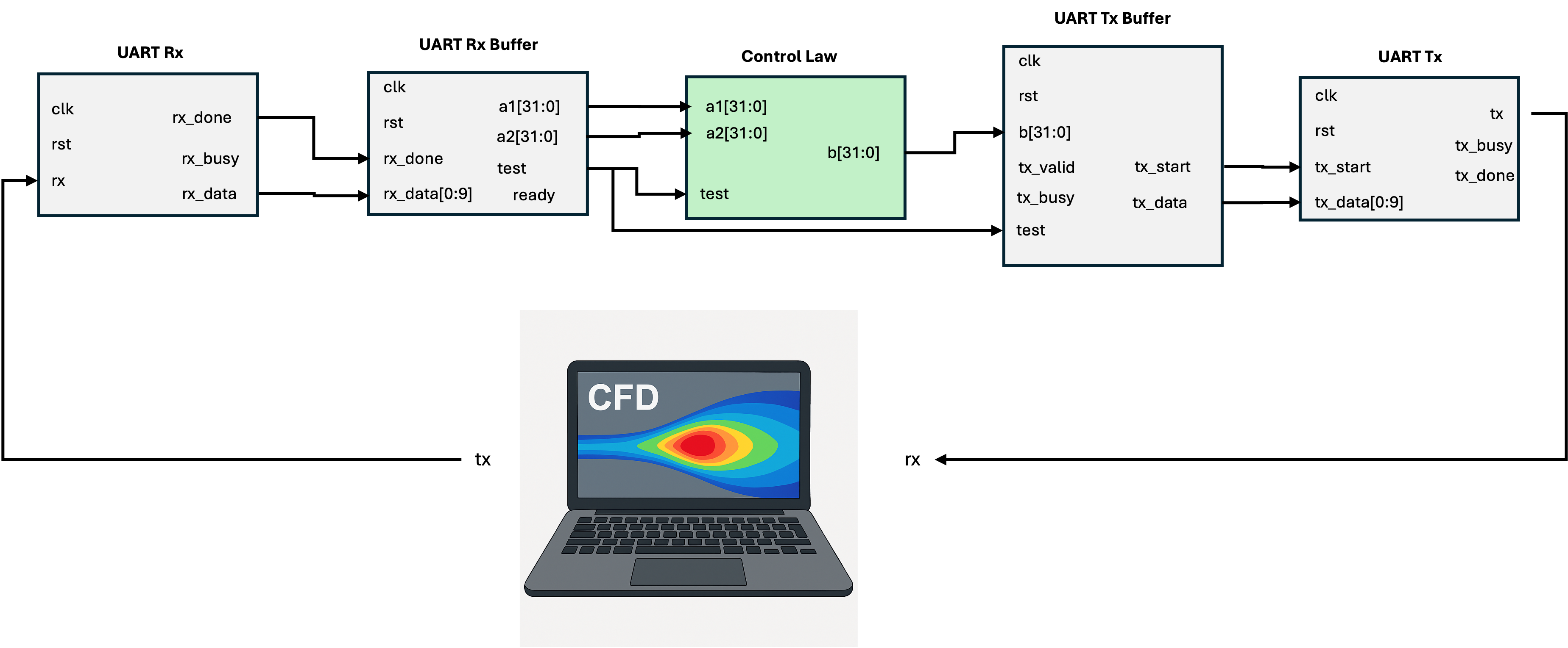
By now, we have a clear picture of the different blocks needed to make this work. From an FPGA perspective, I need to build five blocks (six if we count the top-level module) and integrate them with a simulation of the Landau oscillator. Easy, right? Well… not so much, but that’s the challenge.
The next sections will walk through the development of the FPGA blocks and the Python-based simulation interface.
3. FPGA: Building, simulating, and synthesizing the blocks
3.1 Building and simulating the blocks
My chosen HDL is Verilog since it’s the standard in the USA and I like its simplicity. To keep things straightforward, my modules are pure Verilog (no SystemVerilog for now), and I avoid using IP cores unless absolutely necessary.
The five blocks to build are:
- UART Rx
- UART Rx PID Buffer
- Control Law
- UART TX PID Buffer
- UART TX
All of these blocks are connected through a top-level module.
The final setup will look like this:
Concurrently, once a block is built, it is simulated and tested. For this, I use cocotb. Its Python interface and pytest integration make it far easier to work with than traditional Verilog testbenches.
3.1.2 UART Rx module
There isn’t much mystery in building a UART Rx—there are plenty of examples online. You can check my implementation here. It includes configurable parameters like baud rate and frame size.
The verification phase is handled with cocotb; the testbench is available here.
3.1.3 UART Rx PID Buffer module
This module, UartRxPidBuffer,is responsible for reconstructing two 32-bit fixed-point control inputs (a1 and a2) from UART packets using a custom framing protocol. Each value is transmitted in four separate packets, and the expected structure is:
| START_FRAME | PID | VALUE | END_FRAME. |
Each byte is associated with a specific PID that identifies which part of a1 or a2 it belongs to. The module uses a finite state machine (FSM)to parse incoming bytes,
capture valid data, and assert a one-cycle ready pulseonce both a1 and a2 are fully assembled.
A special TEST_PID is handled separately, allowing quick injection of test data.
Building this module was particularly challenging. My first approach worked fine in isolated tests, but when integrated at the top level it revealed race conditions and incorrect timing behavior. I had to completely redesign the FSM, add explicit tracking of received byte lanes (a1_written, a2_written), and refine the control logic to guarantee a clean, single-cycle handshake.
The final design is now stable, timing-safe, and cleanly interfaces with the Control Law block.
UART Rx PID Buffer Module (Click to expand)
3.1.4 Control Law module
Once the fixed-point arithmetic was set up, the Control Law module became straightforward to implement.
In this block, k1 and k2 are predefined parameters with static values (for now), while a1 and a2 are inputs passed directly from the UART Rx buffer. The module computes:
The good thing about this block is that it’s purely combinational. That means I don’t need to worry much about timing or clock cycles—the output updates immediately whenever the inputs change.
Verification was also simple, and you can check the testbench here.
3.1.5 UART TX PID buffer
This module takes \(b\) , transforms it into an UART frame as the one on 3.2. It wait for a signal from the UART Rx buffer that tells it to read the value from the control law module.
You can check the code here:
UART Tx PID Buffer Module (Click to expand)
The verification script can be found here
3.1.6 UART Tx
There isn’t much explanation needed here. This is a standard UART Tx module with parameters to configure baud rate, frame size, and other options.
You can check the code here and the verification script here.
3.2 Verifying the top module
After weeks of trial and error, I finally had all the blocks working and started integrating them into a top-level module.
The Verilog implementation itself wasn’t complicated:
Top module (click to expand)
The issue was the verification, if you check the test script, I had to test the normal operation mode and the test mode.
The test mode is activated by a special frame sent by my simulation script to test that at least, the FPGA is alive and talking.
3.3 Synthesizing the modules
With verification complete, the next step was to load the design into the FPGA. This requires generating a bitstream—a binary file that maps the Verilog logic into the FPGA’s resources.
The synthesis process has several steps and varies slightly depending on the FPGA vendor. In my case, I used the open-source toolchain:
- Icarus Verilog for simulation,
- Yosys for synthesis,
- Icestorm for place-and-route and bitstream generation.
3.3.1 The resource problem
Here’s where I ran into trouble. The synthesis report showed over 100% utilization of certain FPGA resources. At that point, I had two options:
- Move to an FPGA with more resources
- Optimize my blocks to use fewer registers
Okay, reach the limit of my fpga utilization... Now, we need to optimize... New day, new problem... pic.twitter.com/MQ0kHH6Yec
— Jaime (@jaimebw) May 22, 2025
I initially tried option 2, but my optimization attempts didn’t reduce usage enough, and it would have required a major redesign. In the end, I went with option 1: migrating to a larger FPGA.
Good news, got 2% better lol https://t.co/tAAnppItog pic.twitter.com/jwQ6i4dz5g
— Jaime (@jaimebw) May 22, 2025
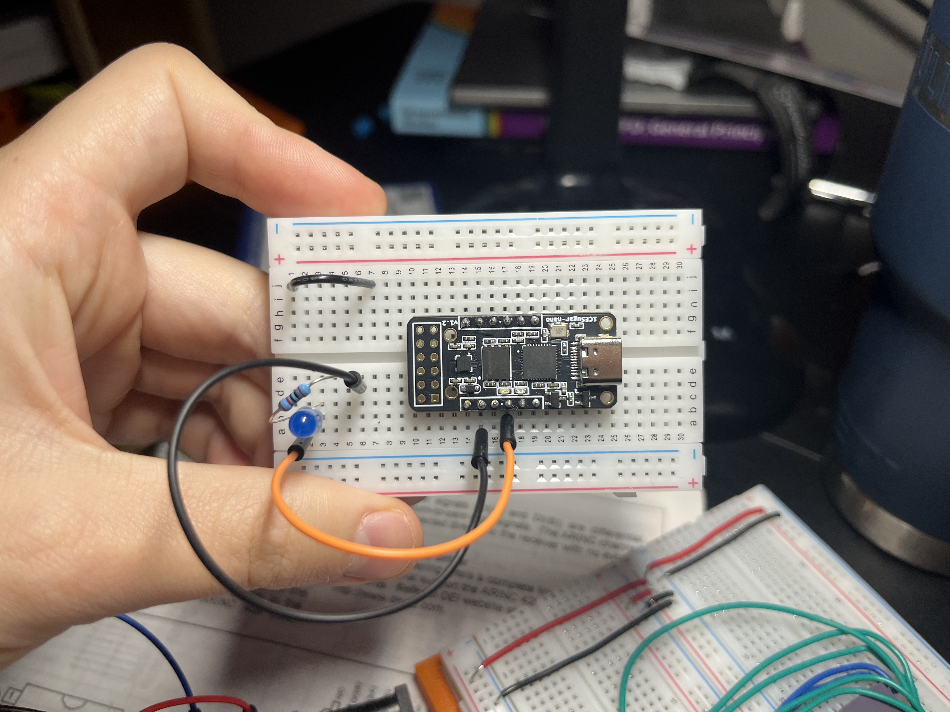
As a reference, you can see the size of the IceSugar nano FPGA in the image below:
4. The change that SoC me!
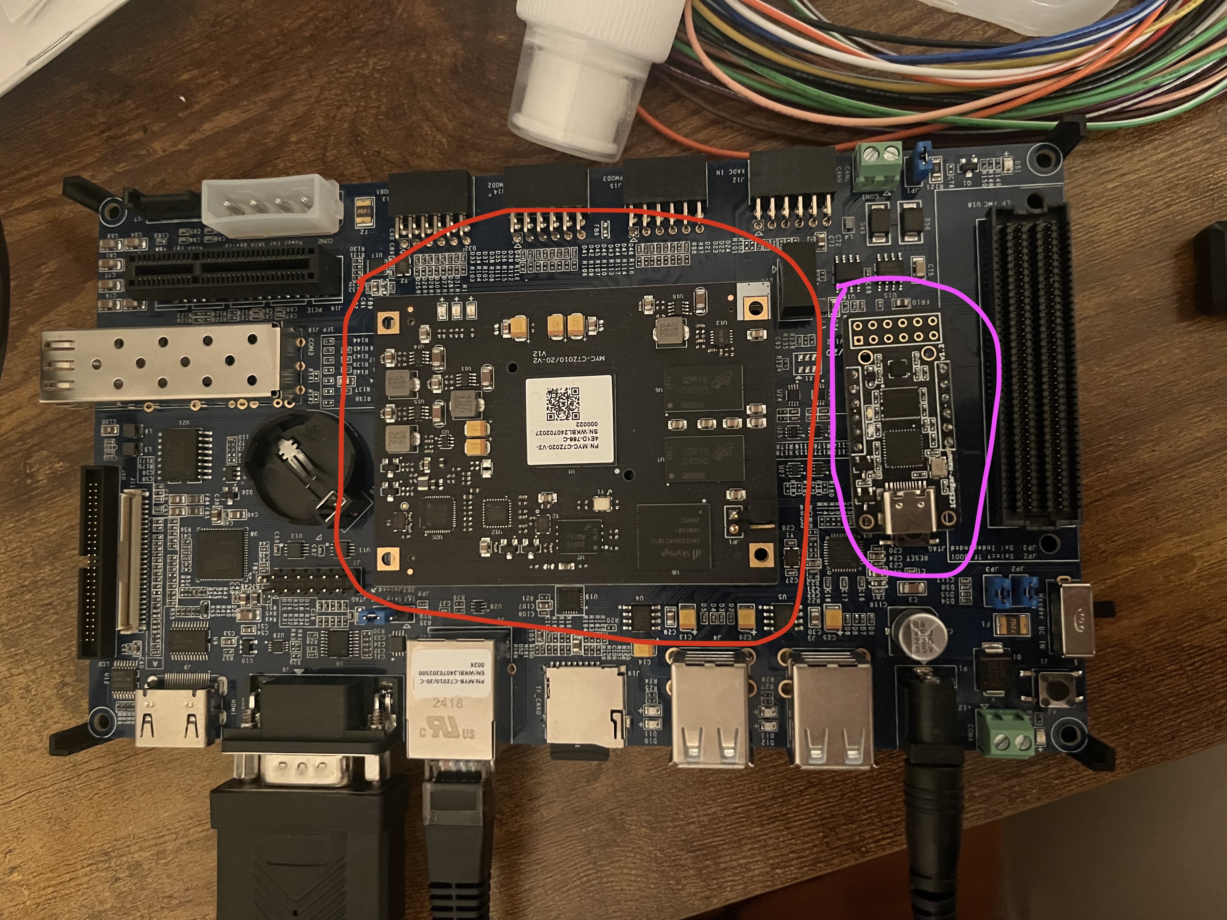
As I hinted in the opening lines, I eventually had to abandon my dream of running everything on the tiny Ice-Nano FPGA. The resource constraints were too tight, and, on top of that, my colleagues were already working with Zynq-7000 SoC boards. The switch made sense: more resources, more flexibility, and the added bonus of tapping into their experience.
This meant I had to revisit two of my earlier questions:
- What is the easiest protocol to interact with an FPGA when it’s integrated into a SoC?
- How do I combine everything into a real hardware-in-the-loop (HIL) experiment?
Below is a comparison in size between the IceSugar Nano and the Zynq7020 SoC:
4.1 What is the easiest protocol to interact with an FPGA integrated with a SoC?
My first thought was to keep using UART, just like in my prototype. I could configure the SoC’s I/O pins, connect through GPIOs, and reuse the design I had already built.
But my advisor Francisco pointed out that this setup was overkill for a SoC. Instead, he suggested I use AXI4—the standard bus that ARM CPUs use to talk to FPGA fabric. AXI4 offered higher throughput, cleaner integration, and a much more scalable solution for my HIL experiments.
So that’s what I did.
For the other research questions, nothing really changed—the only major shift was how the communication was handled.
4.2 New tools, new code and new headaches
This was the start of a whole new learning curve. Suddenly, it wasn’t just about writing Verilog anymore. I had to learn:
- How to use Vivado for synthesis and block design
- How to build and customize PetaLinux
- How to integrate everything into a Zynq SoC workflow
It took time (and a lot of mistakes), but eventually I got over the initial hurdles. The move to SoC was painful, but it opened the door to more powerful experiments.
4.3 Final configuration
After a couple of months of iteration (and plenty of trial and error), I finally reached a stable setup that gave me two key achievements:
- A working PetaLinux build and recipe
- An FPGA bitstream that synthesized and ran successfully
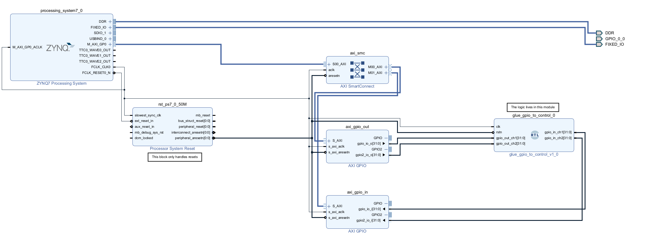
The best part was that I could reuse the Control Law modulefrom my earlier UART prototype. The main challenge was configuring the AXI4 connection between the ARM processor and the FPGA fabric. My approach relied heavily on online resources, combined with guidance from my advisors.
4.3.1 Why AXI4?
The AXI4 interface provides a standardized bus for communication between the ARM core and the FPGA logic inside the Zynq SoC. By implementing AXI4-Lite slave registers, I created memory-mapped control and status registers. This allowed the Linux application running on the ARM processor to directly read and write parameters to the Control Law module.
Compared to UART, this setup offered several advantages:
- No framing overhead → no need to split values into multiple packets
- Higher throughput → AXI4 can run at hundreds of MHz, versus UART’s kilobaud speeds
- Direct memory-mapped access → cleaner integration with Linux applications
The final architecture
The implementation uses Xilinx’s AXI GPIO IP cores to handle the bus protocol details, while my custom Verilog logic connects these registers to the Control Law module.
This architecture cleanly separates the communication interface (AXI4 + ARM) from the computational logic (Control Law in Verilog). That separation makes the design easier to maintain and lets me focus on optimizing the control algorithm itself rather than debugging glue logic.
You can check a snapshot of the block diagram here
4.4 Verification
Here’s the truth: I didn’t perform a formal verification of the AXI4 setup. I took a leap of faith, loaded the bitstream, and assumed it would work on the first try.
Surprisingly enough… it did! 🎉
Sometimes you get lucky in FPGA development, and this was one of those rare moments.
5. Simulating: SoC-Based Closed-Loop Simulation with Hardware-in-the-Loop
With the FPGA logic complete and the move to a Zynq SoC, I had to rethink my entire simulation framework. My original setup used Python (scipy + pyserial) on a laptop to solve the oscillator dynamics and exchange data with the FPGA over UART. Once the design moved onto the SoC, that architecture no longer made sense.
Instead, I rewrote the simulation to run directly on the SoC, using Python to integrate the Landau oscillator equations and the AXI4 interface to communicate with the FPGA fabric in real time.
- At each timestep, Python writes the state variables (
a1,a2) into memory-mapped AXI4 registers. - The FPGA fabric applies the control law and produces the control signal
b(a1, a2). - Python reads the result back through AXI4 and feeds it into the next integration step.
This setup creates a closed-loop hardware-in-the-loop experiment that is now fully self-contained in the SoC. No UART framing, no serial bottlenecks, and no need for multithreaded hacks—just fast, direct memory-mapped communication.
While I lost the convenience of scipy.integrate.solve_ivp, I implemented my own simple integrator in Python (Euler and RK-style methods) to keep the loop running in real time. The tradeoff was worth it: the simulation is leaner, runs directly inside the SoC, and interacts seamlessly with the FPGA logic on every step.
The end result:
Finally made a breakthrough in my FPGA journey . It ain’t much but it’s honest work. pic.twitter.com/b8KfbdRoHe
— Jaime (@jaimebw) September 21, 2025
The real end result
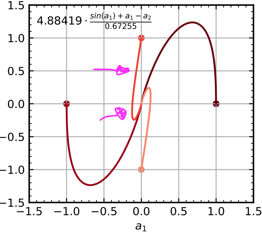
After several iterations — and heavily building on Isaac’s original implementation — I settled on the following control law:
\[b = 4.88419 \cdot \frac{\sin(a_1) + a_1 - a_2}{0.67255}\]Since I wanted to avoid using an FPU on the FPGA, I expanded the sine term using a Taylor polynomial.
To keep resource usage low, I truncated it at the second non-linear term:
This approximation was then ported to fixed-point arithmetic.
You can see the final Verilog implementation here
And with this controller in place, the FPGA successfully stabilizes the system:
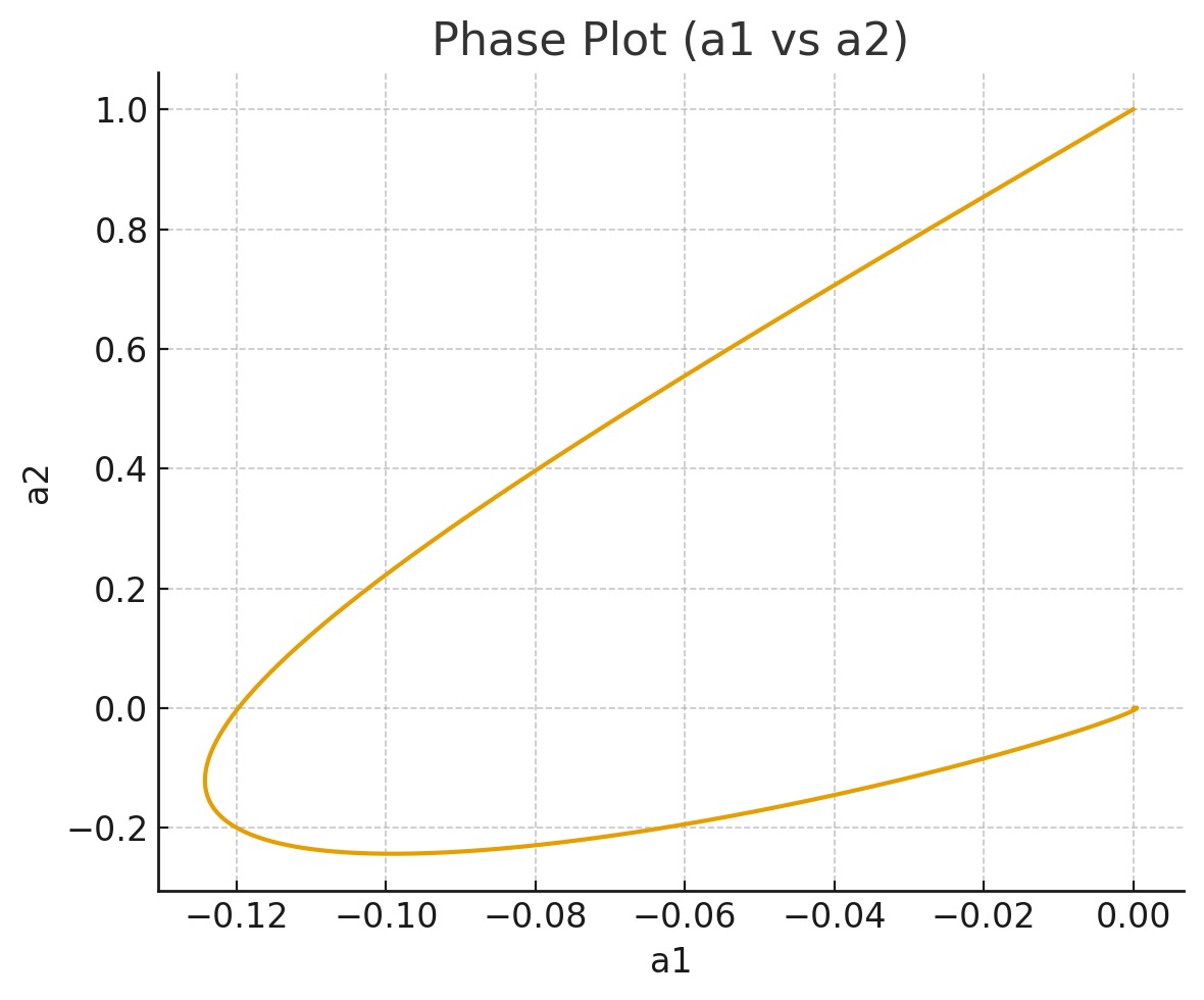
From the phase portrait we observe that both \(a_1\) and \(a_2\) converge to zero and remain there — confirming that the controller is effective.
Below are the reference results from HyGO [1].
The pink curve is the target behavior I should obtain.
However, my implementation deviates from it, likely due to numerical issues introduced by:
- fixed-point arithmetic, and
- the limited-order Taylor approximation of the sine function.
6. Future developments
Looking ahead, my next efforts will be centered on bringing reinforcement learning (RL) into the FPGA. The ultimate goal is to move beyond fixed control laws and enable the hardware to both train and run inference directly in real time. This opens the door to adaptive controllers that can learn and optimize while the system is operating, something especially powerful for active flow control.
In parallel, I plan to extend the simulations toward real CFD calculations. The idea is to start with simplified CFD models and progressively scale up in complexity, always keeping the FPGA in the loop. This combination of RL on hardware and CFD-based environments will push the setup closer to the long-term vision of my PhD: a hardware-in-the-loop digital twin capable of experimenting with flow control strategies under realistic aerodynamic conditions.
References
- Robledo Martin, I. (2025). HyGO: A Python toolbox for Hybrid Genetic Optimization.
- Fixed Point Arithmetic